Purpose
The The RT9081A is a high performance positive voltage regulator with separated bias voltage (VBIAS), designed for applications requiring low input voltage and ultra low dropout voltage, output current up to 500mA. This document explains the function and use of the RT9081A evaluation board (EVB), and provides information to enable operation, modification of the evaluation board and circuit to suit individual requirements.
Introduction
General Product Information
The RT9081A is a high performance positive voltage regulator with separated bias voltage (VBIAS), designed for applications requiring low input voltage and ultra low dropout voltage, output current up to 500mA. The feature of ultra low dropout voltage is ideal for applications where output voltage is very close to input voltage. The input voltage can be as low as 0.8V and the output voltage is adjustable by an external resistive divider. The RT9081A features very low quiescent current consumption for portable applications. The device is available in the ZADFN-6L 1.2x1.2 package.
Product Feature
l Input Voltage Range : 0.8V to 5.5V
l Bias Voltage Range : 2.4V to 5.5V
l 1.5% Output Voltage Accuracy @ 25°C
l Ultra Low Dropout Voltage : 140mV at 500mA
l Low Bias Input Current :
480μA in Operating Mode
40.5μA in Disable Mode
l Enable Control
l Active Discharge Function
l Stable with a 1μF Output Ceramic Capacitor
Key Performance Summary Table
|
Key Features
|
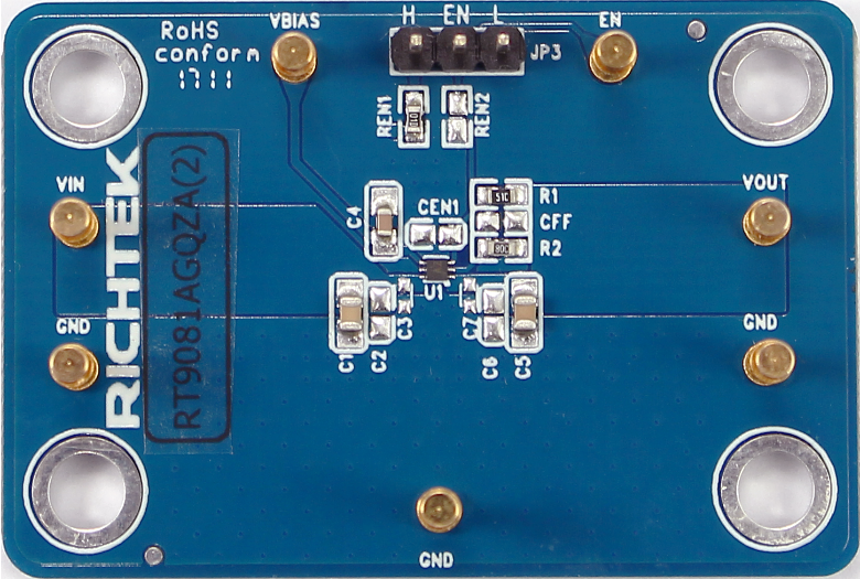
Evaluation Board Number: PCB087_V1
|
|
Default Input Voltage
|
VOUT(Normal) + 0.3V < VIN < 5.5V, VOUT + 1.6V < VBIAS < 5.5V
|
|
Max Output Current
|
500mA
|
|
Default Output Voltage
|
1.2V
|
|
Default Marking & Package Type
|
RT9081AGQZA(2), ZADFN-6L 1.2x1.2
|
Bench Test Setup Conditions
Headers Description and Placement
Carefully inspect all the components used in the EVB according to the following Bill of Materials table, and then make sure all the components are undamaged and correctly installed. If there is any missing or damaged component, which may occur during transportation, please contact our distributors or e-mail us at evb_service@richtek.com.
Test Points
The EVB is provided with the test points and pin names listed in the table below.
|
Test point/
Pin name
|
Signal
|
Comment (expected waveforms or voltage levels on test points)
|
|
VIN
|
Input voltage
|
Power input for the LDO.
|
|
EN
|
Enable test point
|
LDO enable signal input.
|
|
GND
|
Ground
|
Ground.
|
|
VBIAS
|
Power input for the internal control circuit
|
Supply voltage for the LDO control circuit. Mandatory to power up VBIAS before EN and VIN.
|
|
VOUT
|
Output voltage
|
Power output for the LDO.
|
Power-up & Measurement Procedure
1. Connect input power (VVOUT + 0.3V < VIN < 5.5V, VOUT + 1.6V < VBIAS < 5.5V) and input ground to VIN/VBIAS and GND test pins respectively.
2. Connect positive end and negative terminals of load to VOUT and GND test pins respectively.
3. There is a 3-pin header “EN” for enable control. To use a jumper at “H” option to tie EN test pin to input power VIN for enabling the device. Inversely, to use a jumper at “L” option to tie EN test pin and ground GND for disabling the device.
4. Verify the output voltage (approximately 1.2V) between VOUT and GND.
5. Connect an external load up to 500mA to the VOUT and GND terminals and verify the output voltage and current.
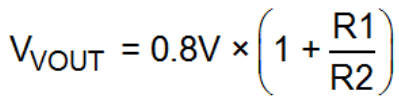
Output Voltage Setting
Set the output voltage with the resistive divider (R1, R2) between VOUT and GND with the midpoint connected to FB. The output is set by the following formula:
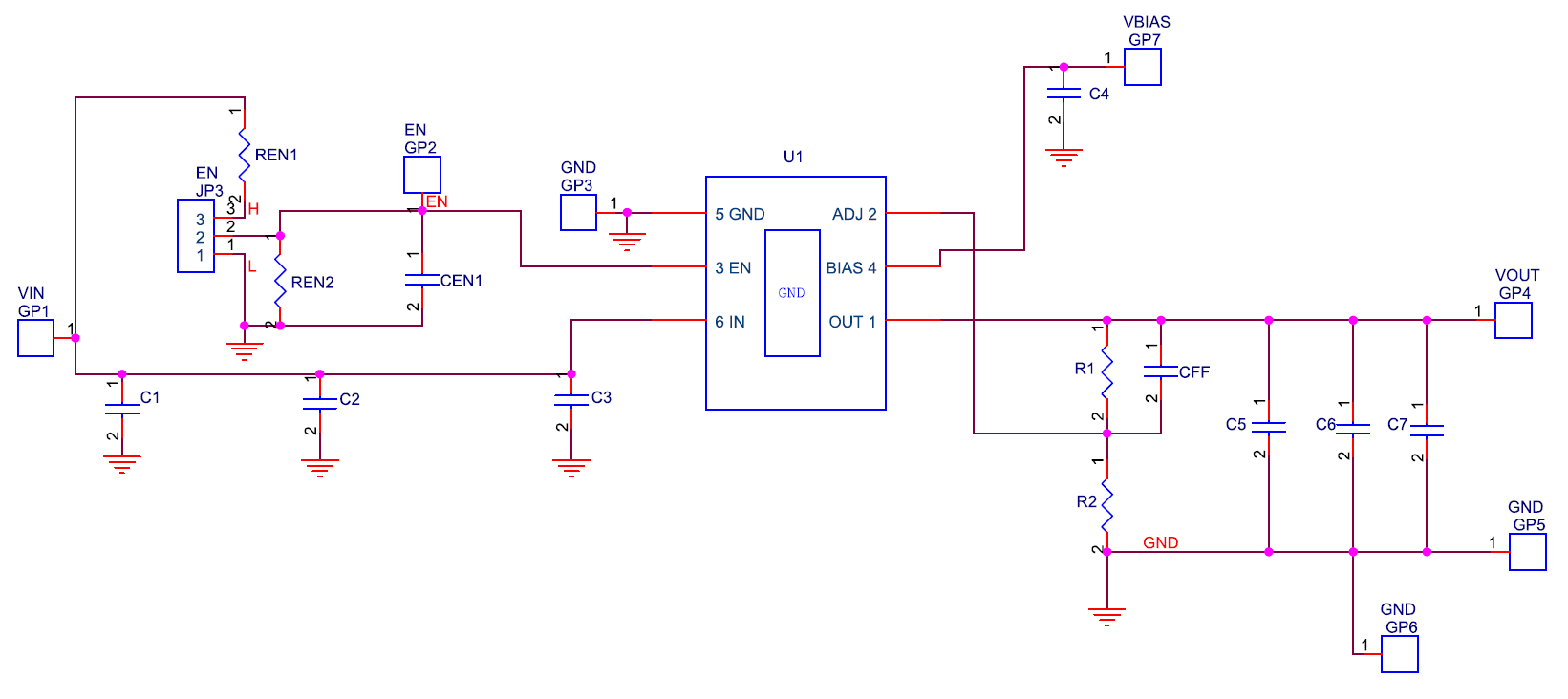
Schematic, Bill of Materials & Board Layout
EVB Schematic Diagram
Bill of Materials
|
Reference
|
Qty
|
Part number
|
Description
|
Package
|
Manufacture
|
|
U1
|
1
|
RT9081AGQZA(2)
|
Linear Regulator
|
ZADFN-6L 1.2x1.2
|
RICHTEK
|
|
C1, C5
|
2
|
C2012X7R1E105KT
|
1µF/25V/X7R
|
C-0805
|
TDK
|
|
C4
|
1
|
C1608X7R1H104K080AA
|
0.1μF/50V/X7R
|
C-0603
|
TDK
|
|
R1
|
1
|
RTT033322FTP
|
33.2k
|
R-0603
|
旺詮
|
|
R2
|
1
|
WR06X6652FTL
|
66.5k
|
R-0603
|
WALSIN
|
|
REN1
|
1
|
WR06X1003FTL
|
100k
|
R-0603
|
WALSIN
|
PCB Layout
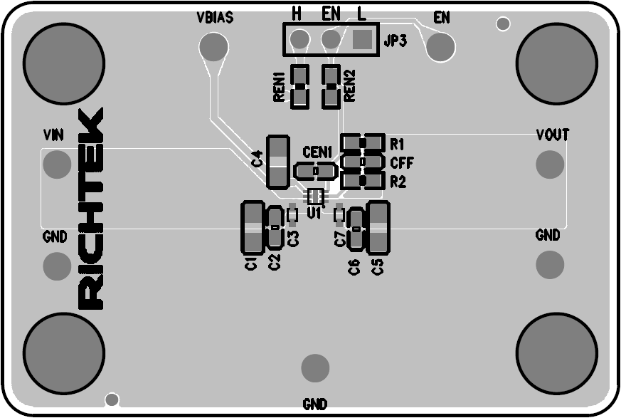
PCB Layout—Top View
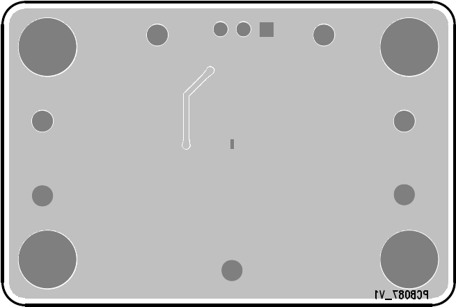
PCB Layout—Bottom View